The place keep-out area (Pad.2) is displayed in transparency.
 |
-
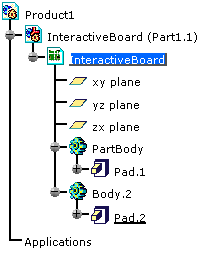
Right-click the Pad.2 in the specification tree and select Properties.
The Properties dialog box opens. -
Click More .
The Circuit Board Design tab appears. 
-
Select the Circuit Board Design tab.
The dialog box is updated as: 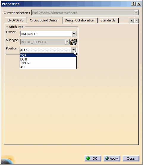
-
Change the position of the constraint area to TOP, BOTTOM, BOTH, INNER, or ALL.
-
Click OK.


This attribute is recognized and displayed in the Circuit Board Design tab.
This attribute is managed only on the idf file import.
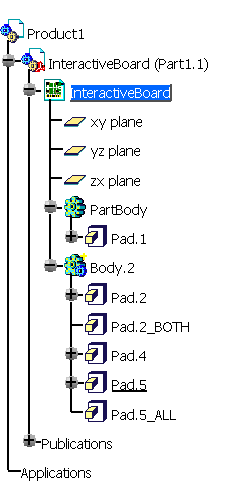
They share the same properties: modifying the properties on one pad will modify them on the other pad. If you change the position of the constraint area from BOTH to TOP or BOTTOM. The node denoting two pads is deleted from the specification tree.
Similarly, if a constraint area has ALL as its position type, a new node is created in the specification tree to denote the same.
 |